| Title: |
A NEW FABRICATION TECHNIQUE FOR INTEGRATING SILICA OPTICAL DEVICES AND MEMS |
| Researchers: |
Karen E. Grutter, Anthony M. Yeh, Susant K. Patra
|
| Funding Agency: |
CIAN, BSAC |
Description:
We have developed a novel fabrication process which integrates silicon MEMS actuators with silica optical components. The suspended silica optical waveguides are actuated by a silicon electrostatic comb drive actuator, with a maximum displacement of 8µm at 50V bias.
There are many potential applications of optical tunable-bandwidth filters in optical communications and signal processing. Using Si photonic MEMS technology, a microdisk filter with a tuning range from 3 to 80 GHz has been demonstrated [1]. Better filter performance can be achieved by using silica as the device material. This has been demonstrated, but the tuning was accomplished using bulk micropositioning stages [2]. In this paper, we report on a novel fabrication process that integrates a silicon-based MEMS comb drive actuator with silica optical components, as shown in Figure 1. To the best of our knowledge, this is the first example of this integration.

Figure 1: Schematic showing the
integration of silicon-based MEMS actuator and silica-only
optical components
Silica is an ideal material for microresonator-based tunable photonic integrated circuits because of its high quality factor (~ 109). However, it is an insulator and integration with MEMS actuators is difficult. Here, we use a modified SCREAM fabrication process [3] on an SOI wafer (Figure 2). The optical components are made from a 1um-thick layer of phosphosilicate glass (PSG) on the SOI. Electrostatic actuation is accomplished through a 25µm-thick silicon layer under the optical components, and electrical isolation is provided by the buried oxide layer. The optical components are protected by photoresist during the deep reactive ion etching (DRIE) step (Figure 2(c)). Upon release (Fig. 2(f)), the silica waveguides and microdisks are completely suspended to avoid substrate leakage. The fabricated device is shown in Figure 3.
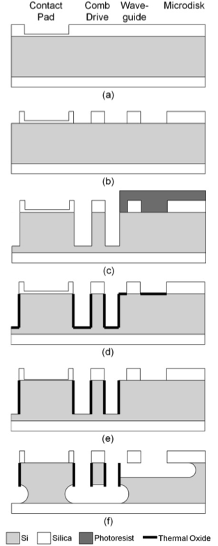
Figure 2: Fabrication process on SOI
wafer. (a) Deposit phosphorus-doped silica and partially
etch MEMS contact pads. (b) Etch device layer. (c) Deep Si
etch with PR protection layer over optical parts. (d)
Remove PR, oxidize Si. (e) Remove floor oxide with
RIE. (f) XeF2 release. After this step, glass can be
reflowed to increase smoothness.
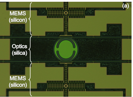 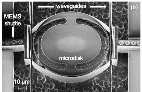
Figure 3: (a) Fabricated device
composed of integrated silica optics and silicon MEMS. (b)
Scanning electron micrograph of device; silica-only
optical components (waveguides, microdisk) are suspended
above substrate while connected to released
silica-on-silicon MEMS (shuttle). Note: the microdisk
includes adiabatic tapering to improve phase matching with
the waveguide.
The suspended optical waveguide has a cross section of 1µm x
1µm. The measured fiber-to-fiber insertion loss of a 1mm-long silica
waveguide is less than 13dB, limited mainly by the coupling loss. The
MEMS combdrive actuator with 20 comb fingers and 3um finger spacing
has a maximum displacement of 8µm at 35V bias. This range of motion is
more than sufficient for our application, in which we predict a
maximum required disk-waveguide distance of 3um in order to achieve a
passband of <1GHz.
We have demonstrated a new fabrication process which integrates silicon MEMS actuators with silica optical components. Our specific device, a tunable-bandwidth filter, demonstrates the use of an electrostatic comb drive to change the coupling of the filter by moving the silica waveguide with respect to the microdisk. Optical performance will be presented at the conference.
|