| Title: |
Optical Antenna Based Nanophotodetector |
| Researchers: |
Ryan Going
|
| Funding Agency: |
Intel; NSF E3S Center |
Description:
Optical interconnects are an increasingly popular solution
for reducing the power consumption of computer chips,
however the full optical link must be much more power
efficient than a metal wire for it to be competitive, likely
below a fJ/bit[1]. In order to reduce the power consumption
of an optical link, the photodetector must be extremely
sensitive, allowing fewer photons to be used per bit of
information. This requires a reduction in capacitance, or
the physical size of the photodiode since the capacitance is
proportional to the linear dimension of the photodiode. For silicon photonics operating at 1500nm wavelength, germanium is commonly used as the detector material for both its CMOS compatibility and optical bandgap near that wavelength. However germanium is a relatively poor absorber at those wavelengths, with an absorption length of over 2 um. An evanescently coupled waveguide photodetector has an even longer length.
To enhance light absorption in a subwavelength germanium region, we
encapsulate the germanium in a metal optical cavity. The key
components include the germanium absorption region, which
forms the bulk of the optical cavity, and has dimensions
which largely determine the resonance. Aluminum encapsulates
the entire cavity to act as both a metal antenna and the
electrical contacts for the device.
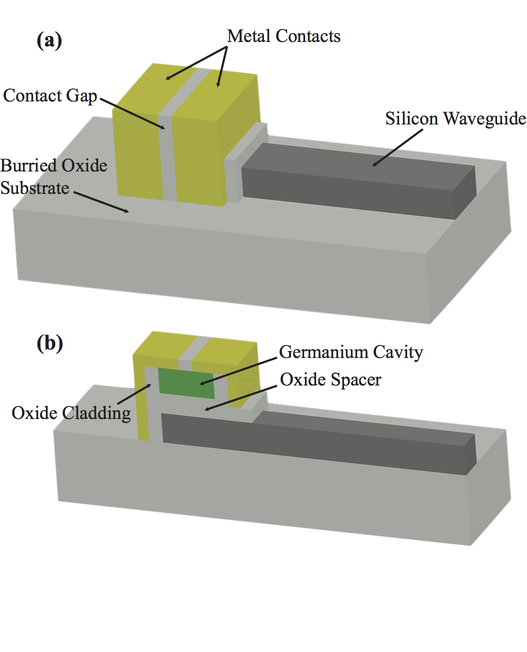
Figure 1: (a) Schematic of metal-clad nanophotodetector coupled to silicon photonic waveguide. (b) Cutaway to show the subwavelength germanium absorption region.
There is a strong single mode resonance produced by this cavity,
which we can couple critically to the waveguide. This
enhances the electric field present in the germanium, and
hence enhances the absorption. Greater than 50% total
absorption can be acheived with this subwavelength size
cavity using CMOS materials and processes.
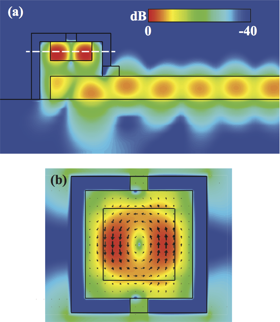
Figure 2: (a) Optical energy density along the center cross-section shows strong enhancement in the germanium cavity. (b) Optical field profile shown for the slice marked in (a) demonstrates the enhancement caused by the gap in the circular doughnut mode.
|