| Title: |
Optical Antenna Based nanoLED / SHE (Spontaneous Hyper Emission) |
| Researchers: |
Michael Eggleston, Seth Fortuna
|
| Funding Agency: |
AFOSR; NSF E3S Center |
Description:
A nanoLED with enhanced spontaneous emission rates will be designed, fabricated, and characterized. The nanoLED will be an attractive option as a light source for future integration into CMOS chips. Its small physical volume, high-efficiency, and fast modulation speeds will enable the use of on-chip optical interconnects that will be able to reduce on-chip energy consumption while allowing for higher clock speeds.
Currently, the size of semiconductor lasers is limited by the diffraction limit of light. In any dielectric cavity, light cannot be "squeezed" into a volume smaller than (λ/2n)3. However, by using charge oscillation in low-loss metals such as gold and silver, it is possible to squeeze optical frequency light into volumes on the order of ~10nm3. By using an optical antenna spontaneous emission can be emitted at a very fast rate. These optical antenna based nanoLEDs will be significantly smaller than traditional laser cavities and therefore ease the integration of these devices for use in CMOS optical interconnects. The small modal volume will also reduce the power consumed by the light emitter. Finally, by using antenna-enhanced spontaneous emission, we will be able to achieve modulation bandwidths greater than 50 GHz at quantum efficiencies approaching and possibly exceeding 50%.
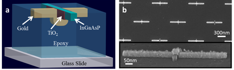
Figure 1: (a) A schematic of the
final design of the optical antenna based nanoLED. The
gain material is etched bulk InGaAsP, the antenna is
formed by a conformal deposition of gold around the gain
material. A 3nm dielectric layer will prevent carrier
recombination from occurring inside the gold. The entire
structure is flip chip bonded to a glass slide with epoxy
and the substrate removed. (b) An SEM micrograph of a
completed array of antennas before bonding to
glass. (inset) A perspective view of an optical antenna
coupled to a ridge of InGaAsP. The ridge is 35nm tall and
30nm width. Dimensions of the gold antenna shown are 50nm
in width, 500nm long, 42nm thick.
Devices with substrates completely removed show enhancement rates of 30x for light polarized parallel to the antenna and total light output increase of almost one order of magnitude. Through these experiments, we have conclusively demonstrated spontaneous emission rate enhancement by eliminating all other possible sources of photoluminescence enhancement.
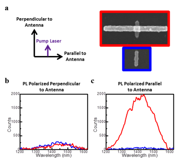
Figure 2: (a) SEM micrographs of bare (blue) and antenna coupled (red) InGaAsP ridge. Arrows indicate polarization direction of PL and pump laser. (b) PL from the structures emitted polarized perpendicular to the antenna (blue - bare, red - antenna coupled). (c) PL from the structures polarized parallel to the antenna.
|