 |
|||
|
|||
| Si-Based Phot. IC's | |
| - overview | |
| - details | |
| - publications | |
| overview | ||||||
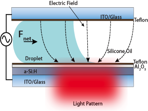
Figure 1: Device schematic showing incident light creates localized areas of high conductivity in the a-Si:H film. This creates localized electric field concentration in the illuminated region resulting in a net electro-mechanical force on the droplet. Fig. 1 illustrates the operating principle of the device. It consists of a microfluidic chamber sandwiched between a photosensitive a-Si:H electrode coated with an electrically insulating oxide layer (bottom) and a transparent electrode (top), a thin hydrophobic layer then coats both surfaces. In the absence of light, the applied AC voltage drops primarily across the highly resistive a-Si:H layer. However, upon illumination, the conductivity of the a-Si:H increases by more than 100x. This causes the voltage to drop primarily across the electrically insulating layer. In other words, the a-Si:H layer acts as a switch that is activated by light which shifts the majority of voltage drop from the photoconductive layer in the "off" state to the dielectric layer in the "on" state. Thus, the illuminated area is analogous to an electrically biased electrode, or a 'virtual electrode'. If the virtual electrode is created only on a fraction of the droplet's contact line, a net electromechanical force acts on the droplet and translates it towards the illuminated region. Fig. 2 and Fig. 3 showcase the capabilities of this device, where parallel movement and array formation of droplets are demonstrated, respectively.
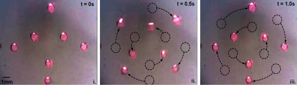
Figure 2: Parallel movement of droplets. 7 droplets undergo simultaneous movement. 4 outer droplets moves clockwise in a circular manner, whilst 3 inner droplets move anti-clockwise in a circular manner.
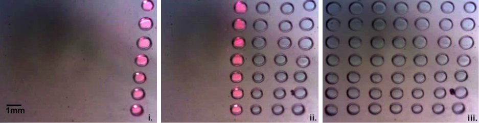
Figure 3:On-demand formation of a parallel array of droplets. Projected light patterns pull seven 200 nL droplets and arrange the droplets into a vertical column before transporting the droplets into a 7x7 array. Movies: Parallel Movement of Seven Droplets |
||||||
| publications | ||||||
|